


The relationship between PCB design and soldering performance has become increasingly critical as electronic assemblies continue to shrink in size whilst growing in complexity. From thermal dissipation to pad geometry, every design decision directly influences solder joint reliability, manufacturability, and long-term operational stability. According to IPC, poor PCB layout practices remain one of the leading contributors to assembly defects in modern electronics manufacturing. Engineers and technicians looking to refine their expertise often pursue training from a master ipc trainer to better understand how design variables affect assembly precision, thermal efficiency, and compliance with global electronics manufacturing standards.
Material Selection and Its Effect on Solderability
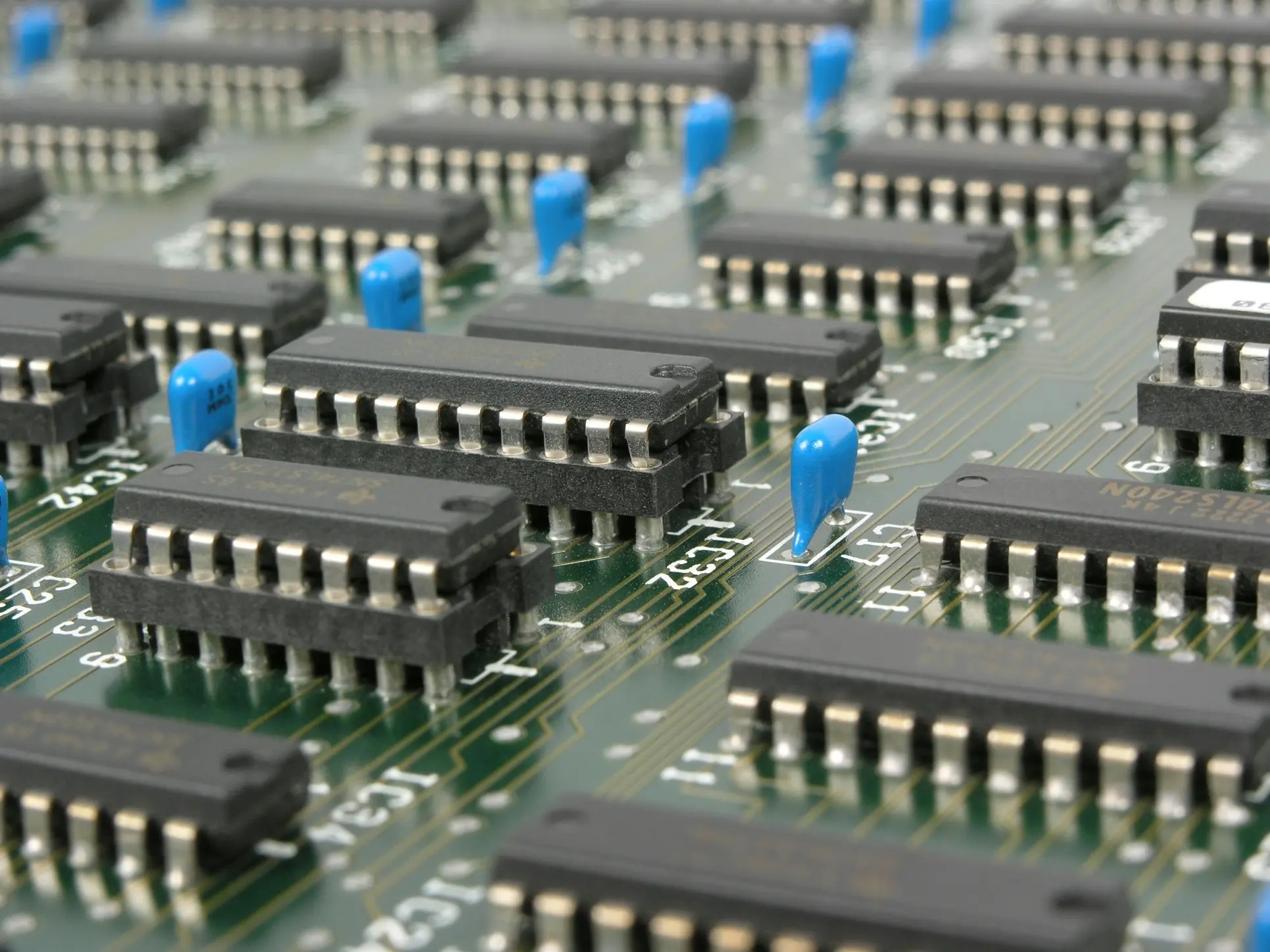
Modern PCB assembly environments demand significantly greater precision than previous generations of electronics manufacturing. Components with ultra-fine pitches, high-density interconnects, and lead-free solder alloys require meticulous board layouts to minimise defects such as solder bridging, insufficient wetting, and thermal stress fractures. Industry standards such as IPC-A-610 establish internationally recognised acceptability criteria for solder joints and electronic assemblies, helping manufacturers maintain consistent production quality and long-term reliability across complex PCB applications.
PCB substrate materials also play a decisive role in soldering performance during assembly procedures. FR-4 remains the dominant laminate due to its mechanical stability and cost-efficiency, whilst advanced applications increasingly utilise polyimide and PTFE-based substrates for superior thermal resistance. According to research presented by the SMTA International Conference, inappropriate surface finish selection can reduce solder joint reliability by more than 20% in thermally demanding environments. These material considerations directly influence heat transfer, solder flow characteristics, and the overall durability of electronic assemblies throughout their operational lifespan.
Pad Geometry, Land Patterns, and Solder Joint Integrity
Pad geometry and land pattern design directly influence the mechanical strength and electrical reliability of solder joints within PCB assemblies. Oversized pads can result in excessive solder deposition and bridging, whilst undersized pads may create weak interconnections due to insufficient wetting. As electronic components continue to decrease in size, particularly within surface-mount technology applications, precision land pattern calculations have become increasingly important for maintaining assembly consistency and reducing manufacturing defects.
Engineers must also account for solder mask clearance, stencil aperture dimensions, and component tolerances when designing PCB layouts for manufacturability. Careful optimisation of pad spacing and solder fillet formation helps improve component alignment during reflow processes whilst reducing the likelihood of assembly defects. By implementing IPC-compliant land pattern standards and refining PCB layout precision, manufacturers can improve solder joint integrity, thermal cycling resistance, and long-term operational reliability.
Thermal Management in PCB Design and Its Role in Soldering
Thermal management remains one of the most technically demanding aspects of PCB design, particularly within multilayer assemblies and high-power electronic applications. Uneven heat distribution during soldering can create excessive thermal stress within solder joints, increasing the risk of component warping and long-term reliability issues. To improve soldering consistency, PCB designers often implement thermal relief pads, balanced copper distribution, and strategically positioned via arrays to regulate heat transfer across the board. These thermal optimisation techniques help improve solder flow, enhance component stability, and minimise assembly defects throughout modern PCB manufacturing processes.
Common Design-Induced Soldering Defects and Mitigation Strategies
Many soldering defects originate during the PCB design stage rather than the assembly process itself. Issues such as tombstoning, solder bridging, insufficient wetting, and component misalignment are frequently linked to poor pad symmetry, inadequate spacing, or inconsistent thermal distribution across the board. As PCB assemblies become increasingly compact and component densities continue to rise, even minor design inconsistencies can significantly affect soldering precision and manufacturing reliability.
To minimise these issues, manufacturers often adopt Design for Manufacturability (DFM) principles during PCB development. DFM-focused layouts improve assembly efficiency by optimising component orientation, spacing tolerances, and thermal balancing before production begins. Combined with automated design rule checking and accurate stencil design, these strategies help reduce rework requirements whilst improving first-pass yield rates and overall solder joint consistency across complex electronic assemblies.
The Role of IPC Standards in Ensuring Soldering Performance
IPC standards establish globally recognised benchmarks for PCB assembly quality, solder joint acceptability, and manufacturing consistency across the electronics industry. Standards such as IPC-A-610 and IPC-J-STD-001 provide detailed guidance on soldering workmanship, component placement, cleanliness, and inspection criteria, helping manufacturers maintain reliable assembly processes within highly demanding electronic applications.
Training centred around IPC methodologies allows engineers, inspectors, and assembly technicians to develop a stronger understanding of defect prevention, soldering best practices, and quality assurance procedures. These standards are particularly important within sectors such as aerospace, automotive, medical electronics, and defence manufacturing, where solder joint reliability and long-term operational stability are critical requirements throughout the product lifecycle.
Design for Manufacturability (DFM) in PCB Assembly
Design for Manufacturability has become an essential engineering principle within modern PCB production, ensuring that board layouts are optimised for efficient assembly and consistent soldering performance. DFM strategies focus on improving component placement, thermal balancing, spacing tolerances, and accessibility for automated assembly equipment. By considering manufacturing limitations during the design stage, engineers can significantly reduce production complications and improve overall assembly precision.
Close collaboration between PCB designers and assembly specialists also plays an important role in successful DFM implementation. Early-stage manufacturability reviews help identify potential soldering challenges before production begins, reducing unnecessary rework and improving process efficiency across complex electronic assemblies. As PCB architectures continue to evolve towards higher-density configurations, DFM methodologies remain critical for maintaining solder joint reliability, production consistency, and long-term product performance.
Conclusion
PCB design and soldering performance remain fundamentally interconnected within modern electronics manufacturing. From material selection and pad geometry to thermal management and manufacturability optimisation, every design decision directly influences solder joint reliability, assembly consistency, and long-term operational performance. As electronic systems continue advancing towards increasingly compact and complex architectures, the importance of robust PCB design practices and adherence to IPC standards will remain essential for achieving high-quality, reliable electronic assemblies across the global technology sector.